A photograph of the Leica electron beam lithography tool is pictured here. For more details, visit the website for Ohio's Nanoscale Patterning Consortium.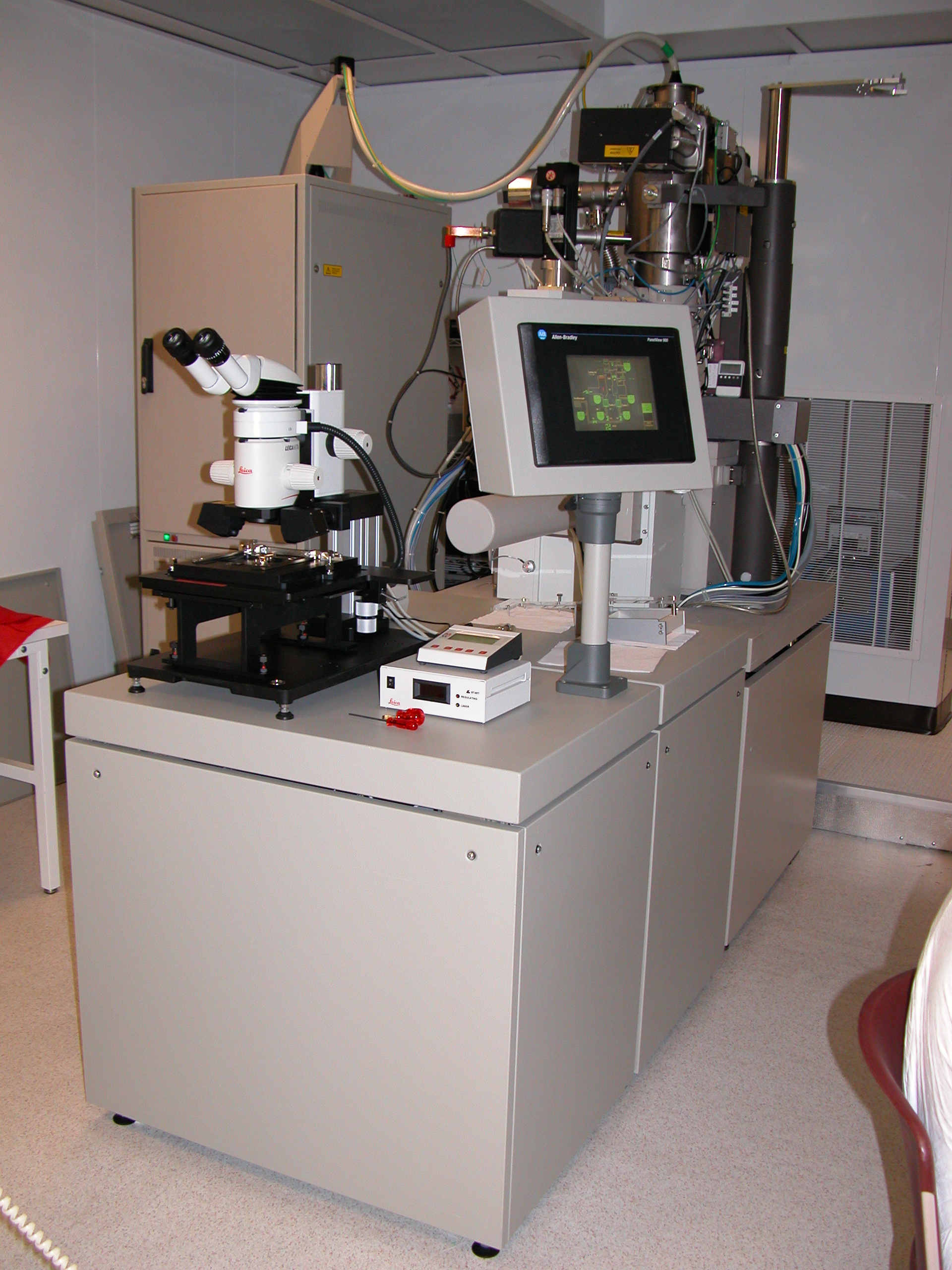
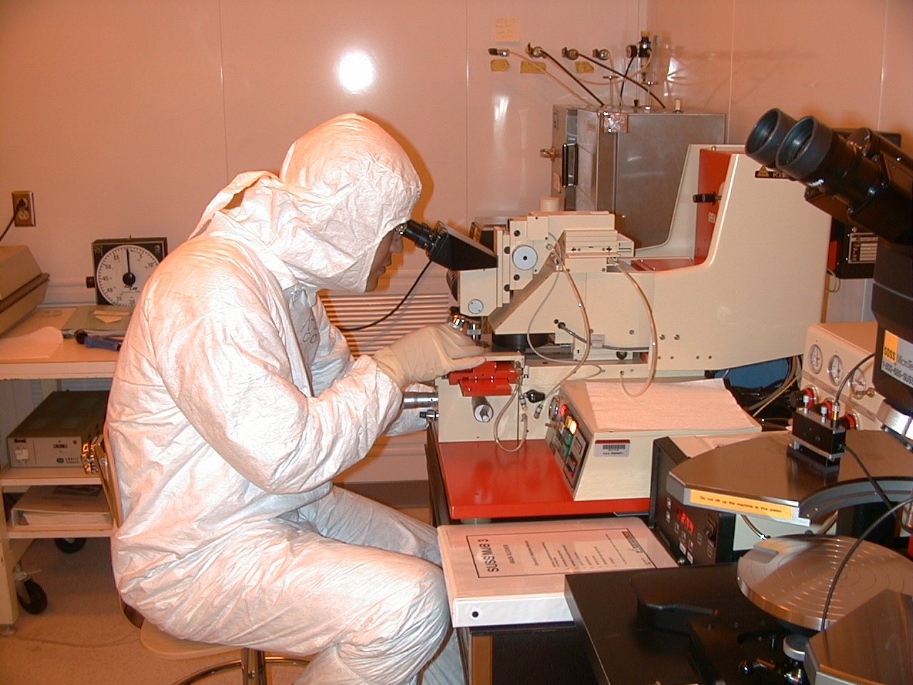
Berger has contributed greatly to the infrastructure of the shared cleanroom facility. Some specific items in the shared cleanroom belonging to the Berger research group are: the Karl Suss MJB3 mask aligner, (shown below); Leitz Ergolux optical microscope with CCD camera acquisition and phase contrast capability (shown below), and a programmable hotplate for precise photoresist baking.
Sung-Yong Chung demonstartes the capabilities and high resolution of the ultraviolet MJB3 contact mask aligner. Our group's prior results have achieved metal lines as narrow as 0.7 microns, and routinely down to 1-2 microns.
Sung-Yong Chung illustrates the usefullness of quick inspection of samples in between process steps using the Leitz Ergolux optical microscope with CCD camera acquisition and phase contrast capability.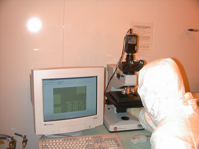
Finally, in a joint NSF equipment grant, Berger acquired an Oxford inductively-coupled plasma reactive ion etching (ICP-RIE) system. It has 8 gas lines for Cl and F chemistries and dedicated liners for each chemistry. The ICP-RIE temperature controlled stage provides a large process window from cryogenic temperatures up to 400 C.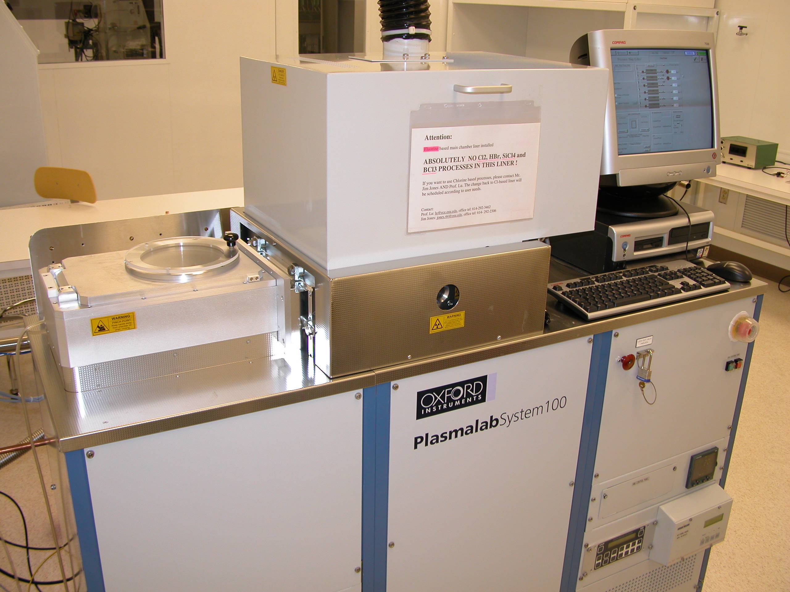
In addition to ECE faculty, staff and students, the facilities are available to researchers from Physics, Material Science, Chemical Engineering, Chemistry, Mechanical Engineering, Welding Engineering and from outside Ohio State University. Arrangements for access by non-ECE Department personnel can be made by contacting Cleanroom Supervisor James Jones.
Berger's Nanoelectronics and Optoelectronics Lab (NOEL) that includes a complete electrical measurement system for probing ultra-small features with an Alessi REL-4830HT probe station with a guarded chuck using a combination of four triaxial MH2-B probes and two more coaxial MH2-B probes. Each probe has a one micron resolution. The test setup can perform DC and pulsed I-V measurements from femtoamperes to amperes (HP 4156C Parameter Analyzer with Option 410 Expander chassis). The expander chassis permits high current measurements up to 1 A, beyond the 100 mA compliance of the 4156C parameter analyzer. The probe station is equipped to handle a temperature range of 0-300C. C-V measurements are also possible with a Materials Development system that includes an HP 4284 LCR meter with an bias-T to force up to 100 V biases.
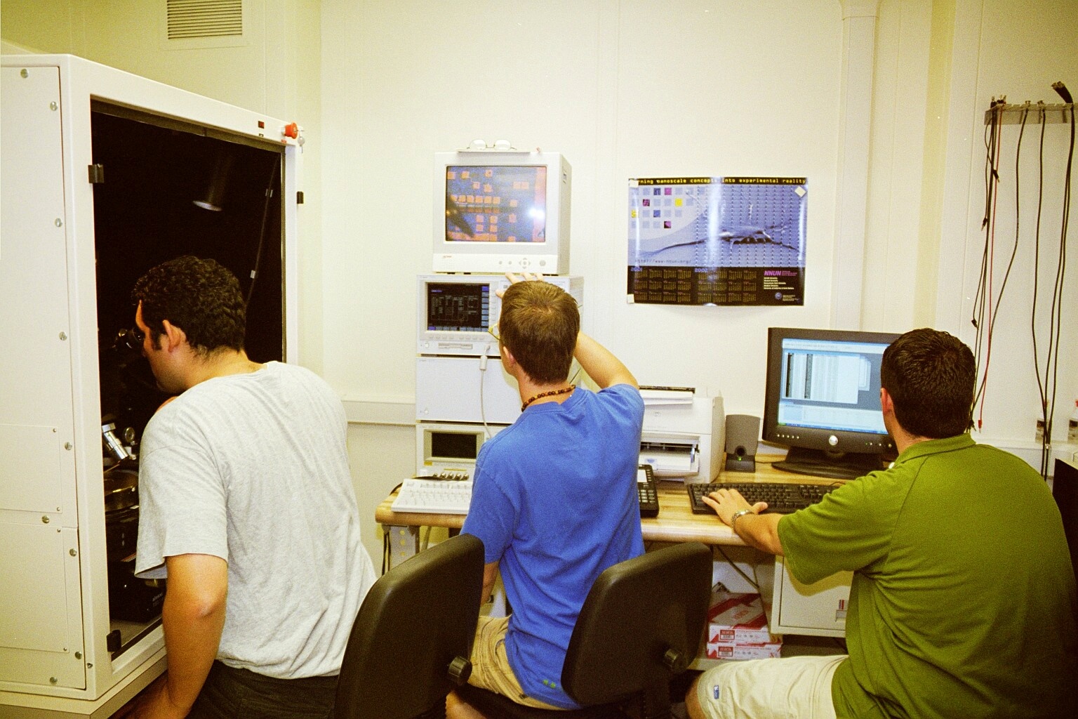
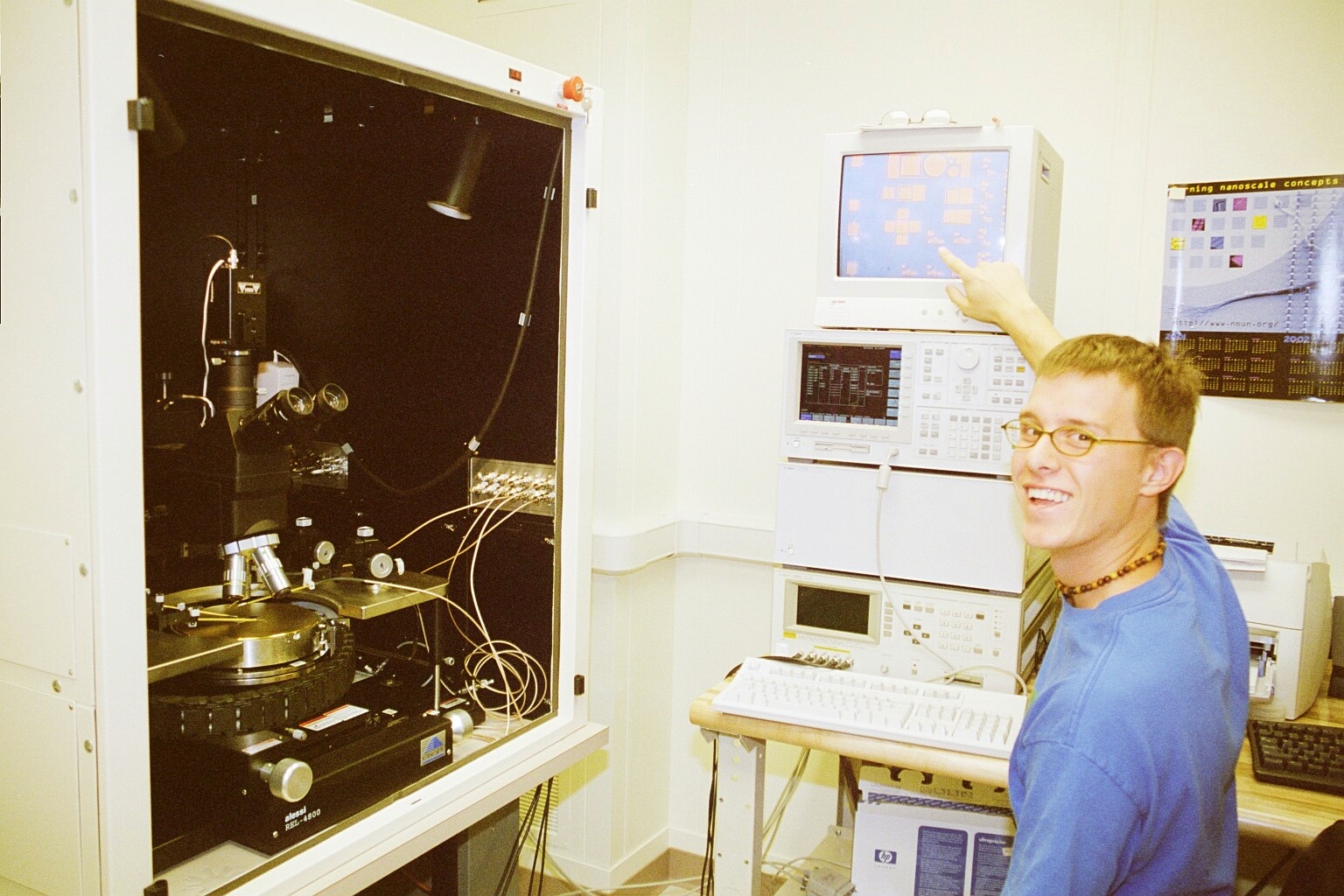
Ryan Pavlovicz (undergraduate researcher) indicates the devices he is probing on the screen using the probe station for current-voltage measurements.
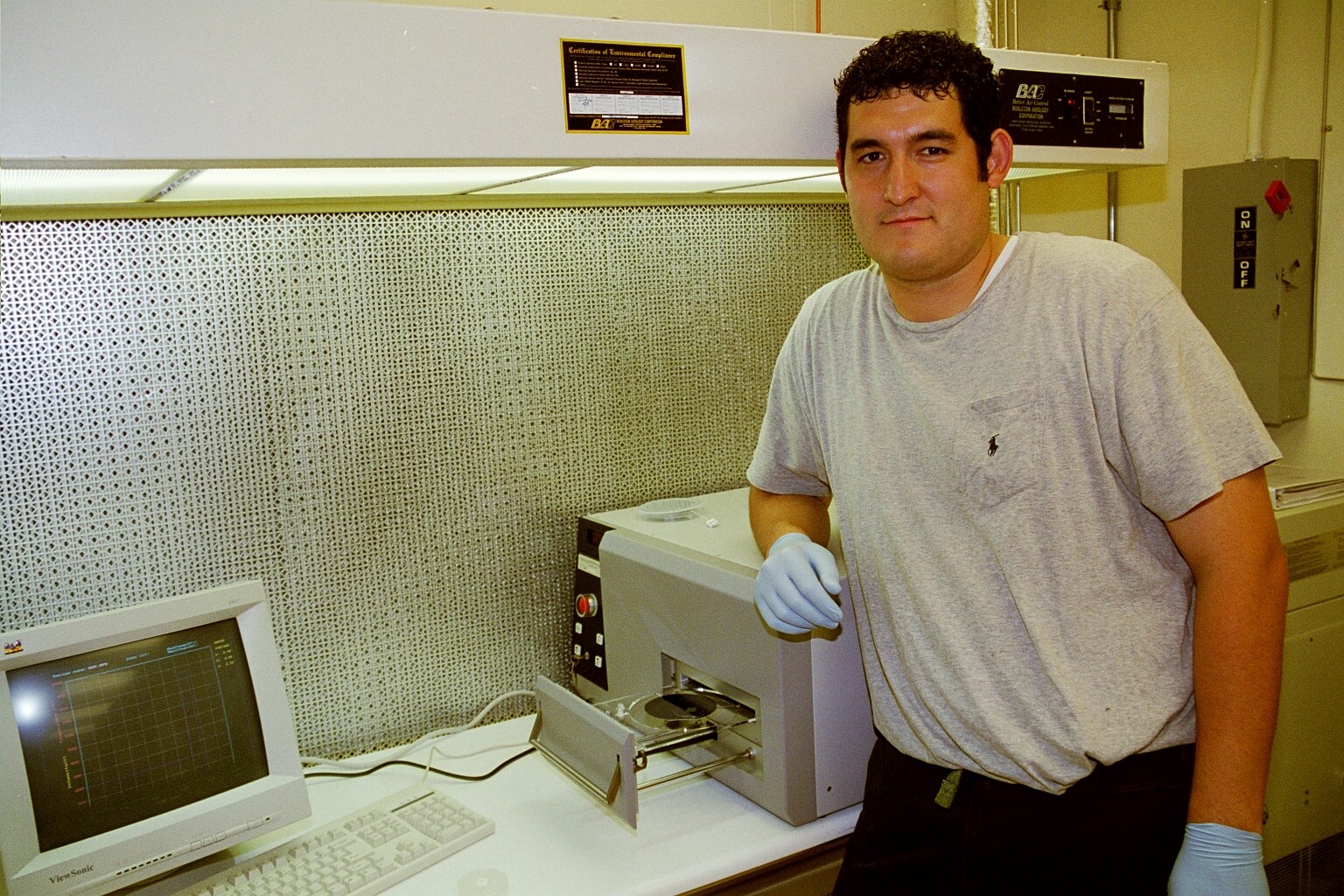
Tony Rice shows the Modular Process Technology's RTP-600S rapid thermal annealing system with a temperature range of 350-1300C plus/minus 2C as monitored by either a thermocouple or dual-color pyrometer. Samples sizes up to 6-inches can be accommodated. Real-time process sampling every 100 msec provides recipe validation. A Neslab HX-300 water chiller supports the cooling of the chamber.
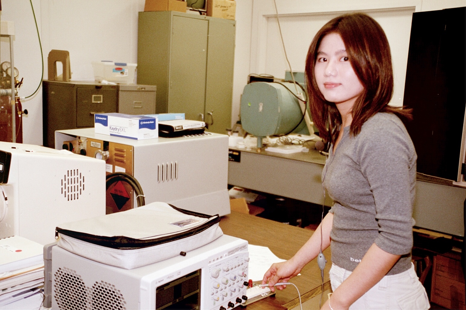
Ms. Inge Tansu (undergraduate researcher) demonstrates the oscilliscope with voice recognition software.
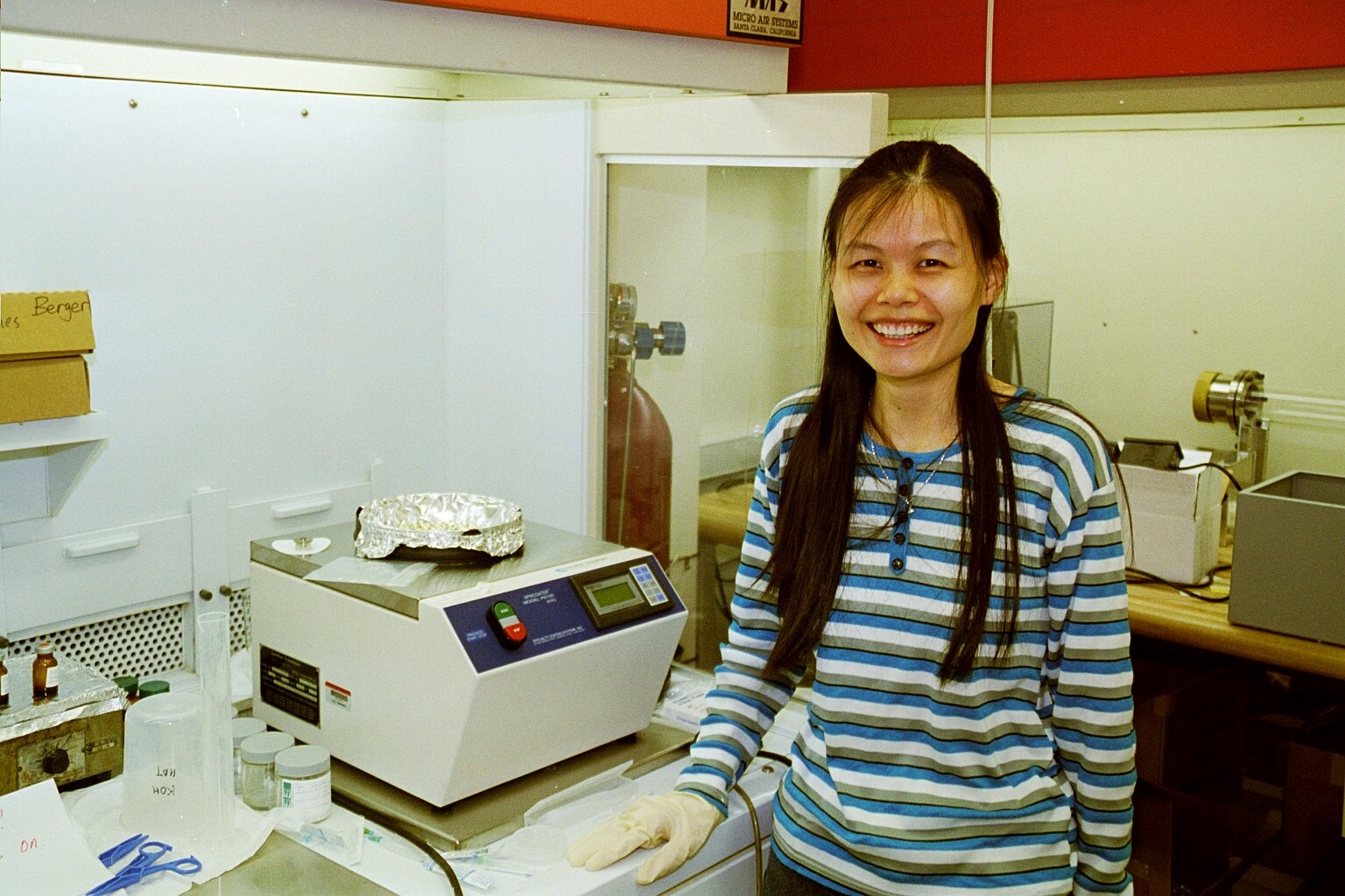
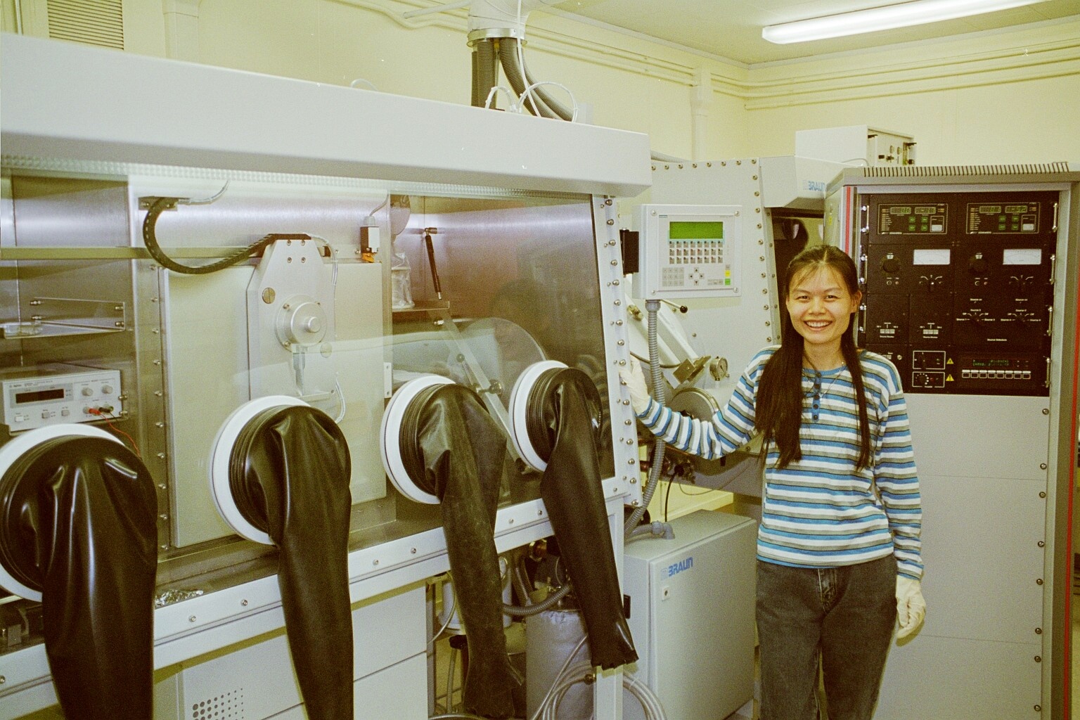
Berger's Polymer Device Laboratory (PDL) is equipped with a glovebox system for the synthesis of polymeric devices by separate spin coating and metallizations within an inert ambient. The system was supported by an NSF Instrumentation for Materials Research (IMR) award (DMR-0196040). The installed glovebox system includes an MBraun LabMaster 130 (1500 mm w/ 3 ports) with solvent removal and a Specialty Coating Services spin coater (SCS P6708). Connected to the spinner glovebox is an MB200 Workstation (1800 mm w/ 4 ports). Enclosed within the MB200 is an MBraun vacuum system that features a BOC Edwards Auto 500 thermal evaporator with a 6-pocket thermal source and pumped by a 500 l/s turbo molecular pump backed by a dry scroll pump. The vacuum system also features dual pneumatic doors for easy access either from inside or outside the glovebox system (Fig. 3). Three quartz crystal monitors and two separate current sources enable the co-deposition of two source materials to be independently controlled and monitored. The PDL is also equipped with a second SCS-P6708 spin coater external to the glovebox for non-sensitive spinning, a tube furnace for baking (vacuum or nitrogen ambient), Tegal Plasmaline 415 plasma asher, Veeco Dektak^3 profilometer, microbalance and Rudolph Auto-EL III ellipsometer. Featured above is a fume hood with spin-coater. Here, Ms. Yifan Xu shows the spinner in the fume hood.
Ms. Yifan Xu shows the MBraun glovebox with spin-coater and the in-situ testing with the portable Keithley 4200 parameter analyzer..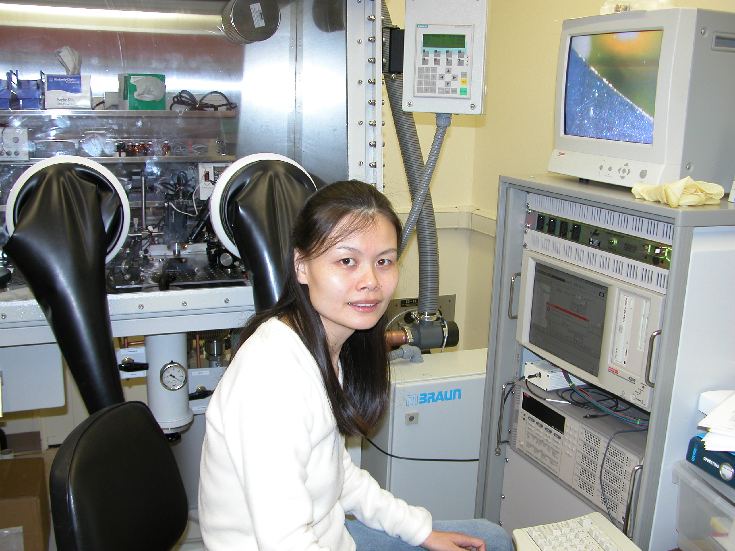
Ms. Yifan Xu shows the MBraun glovebox with a built-in Edwards thermal evaporator for deposition of reactive metals.
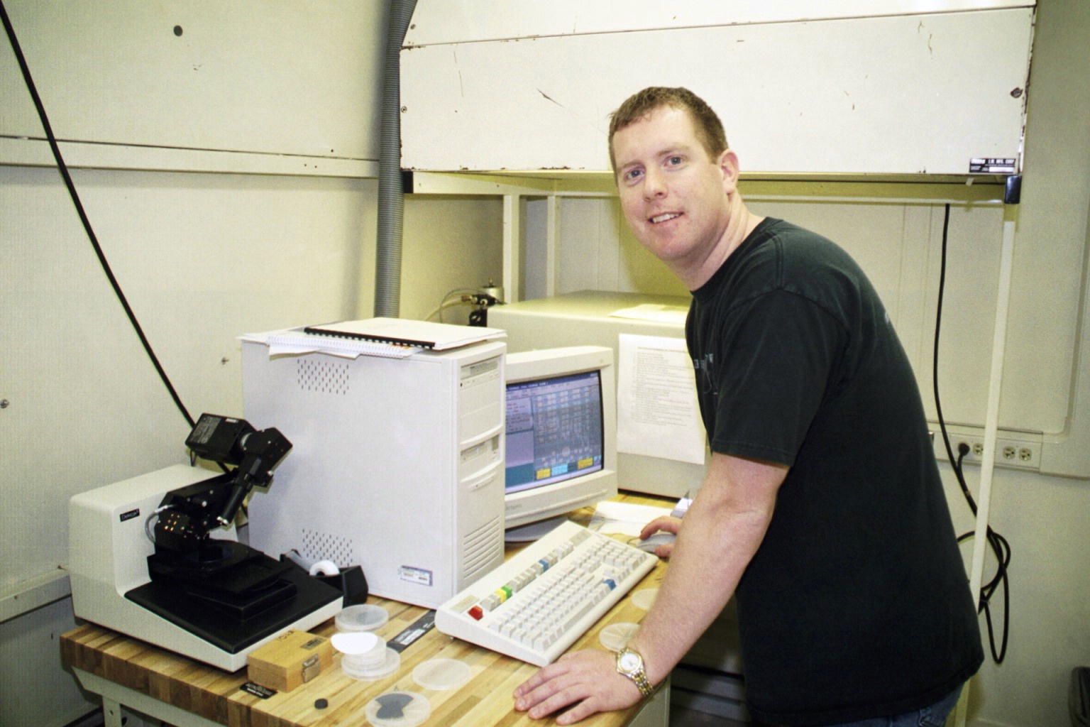
Here Ms. Yifan Xu shows the Rudolph Auto EL single-wavelength ellipsometer system for measuring thin dielectrics.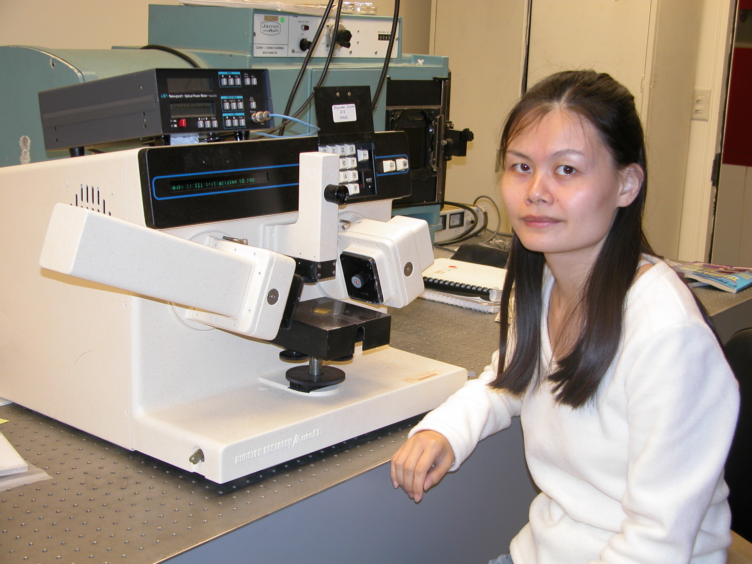
Matt Williams (undergraduate researcher) shows the Veeco Dektak^3 profilometer for measuring film thickness to 5 nm precision.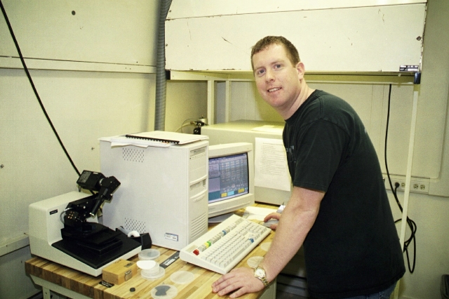
Last updated February 5, 2006.