
The OSU Nanoscale Patterning Laboratory:
Part of the the Nanofabrication and Materials Processing Center (NanoMPC)
 |
Paul R. Berger
Professor and Founder
Campus Address:
201 Caldwell Laboratory
Mailing Address:
Department of Electrical and Computer Engineering
The Ohio State University
205 Dreese Laboratory
2015 Neil Avenue
Columbus, OH 43210 USA
Direct phone: (614) 247-6235
EE Dept. FAX: (614) 292-7596
Email: pberger@ieee.org
|
 |
Aimee L. Price
Senior Research Associate
Electron Beam Lithography Engineer
Campus Address:
Mailing Address:
The Ohio State University
218 Science Village
1381 Kinnear Road
Columbus, OH 43210 USA
Direct office phone: (614) 292-2753
Email: price.798@osu.edu
|
Please note that the EBL system was moved to its new location at
Nanotech West on west campus
along Kinnear Road.
The IMR Shuttle services provides hourly access to/from central campus,
door-to-door. The IMR Shuttle schedule cam be found
here.
The move was intended to bring greater access and tool support in order
to accomdadate the growing user base. The Nanotech West facility should
provide a more stable infrastructure leading to reduced tool downtime
and more staff support, although Ms. Bross will still be the principle
point-of-contact for new and current users. Further, the proximity
of a dedicated scanning electron microscope well suited for imaging
nanoscale insulating resists will be added that will certainly improve
and expedite post-development
analysis, providing faster iterations of your experiments. The new SEM
is courtesy of Wright Center of Innvation on
Photovoltaics Innovation and Commercialization (PVIC) which
includes a significant infusion of leading edge process equipment for
semiconductor and related materials. Berger is a key member within PVIC,
developing organic photovoltaics and related materials.
Paul Berger
Relevant Links:
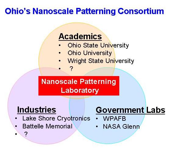
Our first year of operation has already demonstrated a wide and healthy impact upon the Ohio
State community, and beyond, crossing departmental, college, university and state boundaries
(see below).
Introduction:
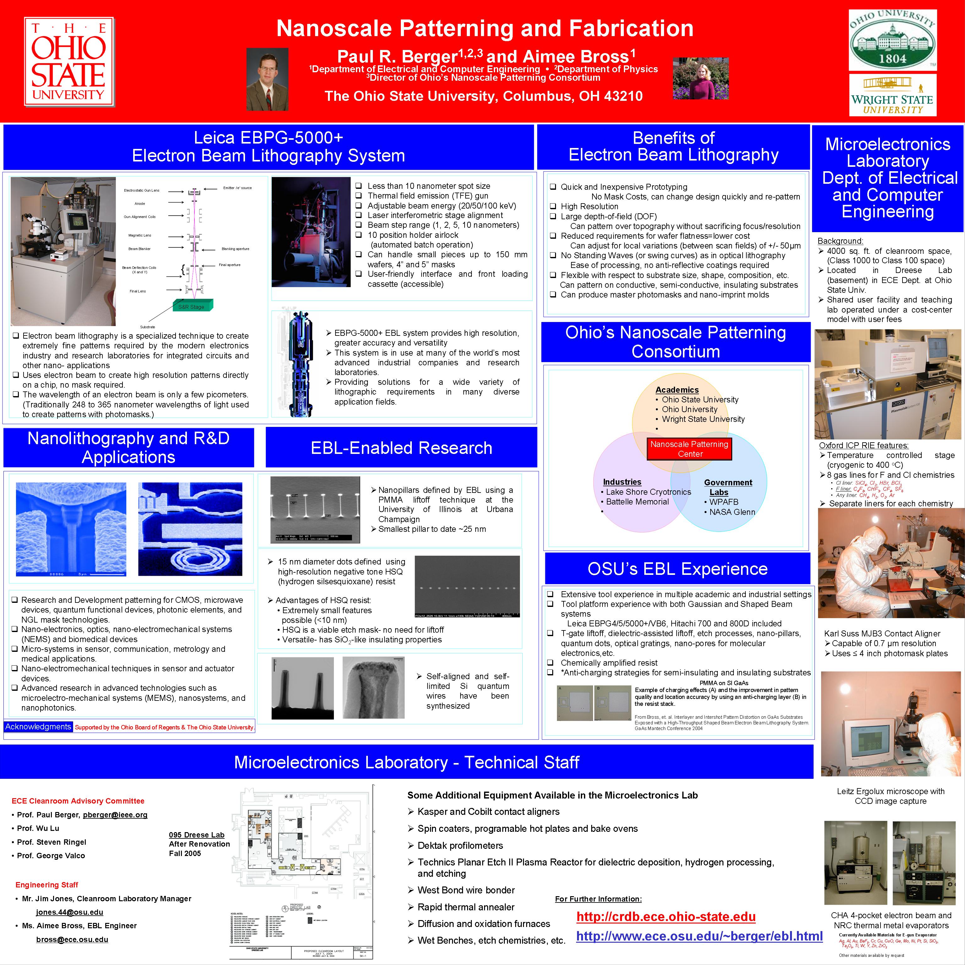
The new electron beam lithography (EBL) facilities are in
the process of being installed into the OSU's Microelectronics Cleanroom Laboratory.
The entire facility was supported by the Ohio Board of Regents and equates to a
multi-million dollar investment by the State of Ohio and the Ohio State University.
The hiring of key university staff with an extensive knowledge of electron beam
lithography in both academic and industrial settings will serve a broad customer
base well to service your individual needs.
In layman's terms, it is a sophisticated tool for patterning samples at the nanometer
scale all the way down to single digit nanometers! Samples can be virtually anything
that can exist in a vacuum, and that has a relatively planar surface.
The process works just like your TV, assuming you do not own a flat-panel set yet.
Your cathode ray tube (CRT) creates an electron beam that is scanned, or rather
rastered, across a phosphor-coated screen by voltage controlled plates, providing
you with a suitable picture image. In our case, the electron beam has a very small
spot size and its position on a sample can be controlled also to single digit
nanometer precision. The sample is coated with a material, generally from a polymer
based solution, that changes its properties when it is exposed to the electron beam.
Then with a process of developing, similar to photography, the exposed image is
developed in a solution. A myriad of other processing techniques can then be performed
to the sample that will alter the samples properties only within the specified regions.
One example of this type of processing is the manufacturing of a computer chip.
Key Features of the Leica EBPG-5000 electron beam lithography system:
- Less than 10 nanometer spot size
- Thermal field emission (TFE) gun
- Adjustable beam energy (20/50/100 KeV)
- Large 127 mm stage travel
- Laser interferometric stage alignment
- Beam step range (1, 2, 5, 10 nanometers)
- Substrate capability up to 150 mm (incl. 4-inch mask plate holder and a piece part holder)
- 10 position holder airlock with a "straight through" loading facility
- User-friendly interface
For further details, see the Leica brochure (2.7 Mb) .
Operational Policies:
The new facility is open to all users, including academic institutions within and outside
Ohio, private companies and government laboratories. The new facility will operate on a cost center model
and will incur user fees to defray operational costs. The staff EBL engineer (see Ms. Bross's contact info above)
will be available to work with outside users for either training users or running your jobs directly. Ms. Bross supervises
the daily operation of the EBL system.
User Forms:
User Fees and Cost Structure:
Please contact the EBL Engineer, Ms. Aimee Bross (contact info above) to determine your needs.
A full cost structure is articulated below and is commeasurate with peer institutions.
- Internal OSU Users - Direct Write
- Direct beam write time, partitioned into 15 minute increments
- Additional OSU Ebeam Staff time (processing, process development, etc):
- External Academic Users - Direct Write
- Direct beam write time, partioned into 15 minute increments,
- Additional OSU Ebeam Staff time (processing, process development, etc):
- External Industrial Users - Direct Write
- Direct beam write time, partioned into 15 minute increments,
- Additional OSU Ebeam Staff time (processing, process development, etc):
- 4-inch Photomasks (flat-rate, depending upon beam-time threshold)
- Internal users, per mask for up to 16 hours beam time,
- External users, per mask for up to 16 hours beam time,
- 5-inch Photomasks (flat-rate, depending upon beam-time threshold)
- To be determined, when a user base requesting this service requires it.
The facility operates as a cost-center and thus fees defray operating expenses. As operating
expenses are a moving target, the users fees will be reviewed annually and altered accordingly.
Layout Formats and CAD Layout Software:
The preferred format for job submission is the standard GDSII, but other formats can be accepted.
Please contact the EBL staff to determine compatibility. For those academic users who do not have
a suitable CAD layout editor, we are looking into providing limited access to software that would
meet your CAD layout needs. We also hope to offer this service to off-site users.
Miscellaneous:
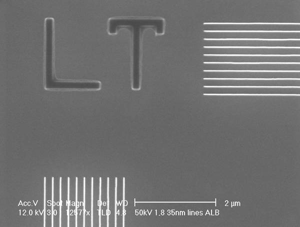
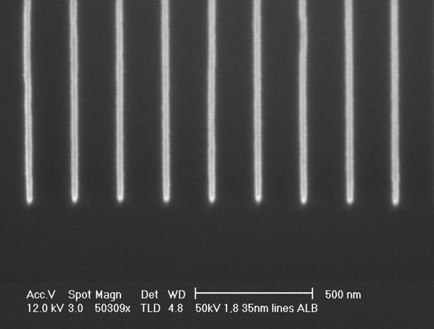
Below are early (12/19/05) photomicrographs of test patterns written during the tool acceptance testing.
Note, that the
field emission source permits a sub-10nm spot size, and thus we have not pushed the system to its lower resolution limit yet.
Work to date has been at coarser resolutions only.
- 35 nm horizontal and vertical lines, 200 nm pitch, HSQ on SiO2
- Exposure: Leica EBPG 5000, 50 kV, 500 pA, 12/19/05
- Resist: 80 nm of HSQ
(OSU thanks E. Kratschmer from IBM Yorktown for donation of HSQ coated Si wafers and M. Rogosky from Penn State University for HSQ)
- Develop: 70 sec 0.26N TMAH, 10 sec in 9:1 H2O:0.26N TMAH, 10 sec H2O rinse, N2 dry
- Image: FEI Sirion SEM 12 kV, UHR (thanks to C. Begg OSU CEOF)
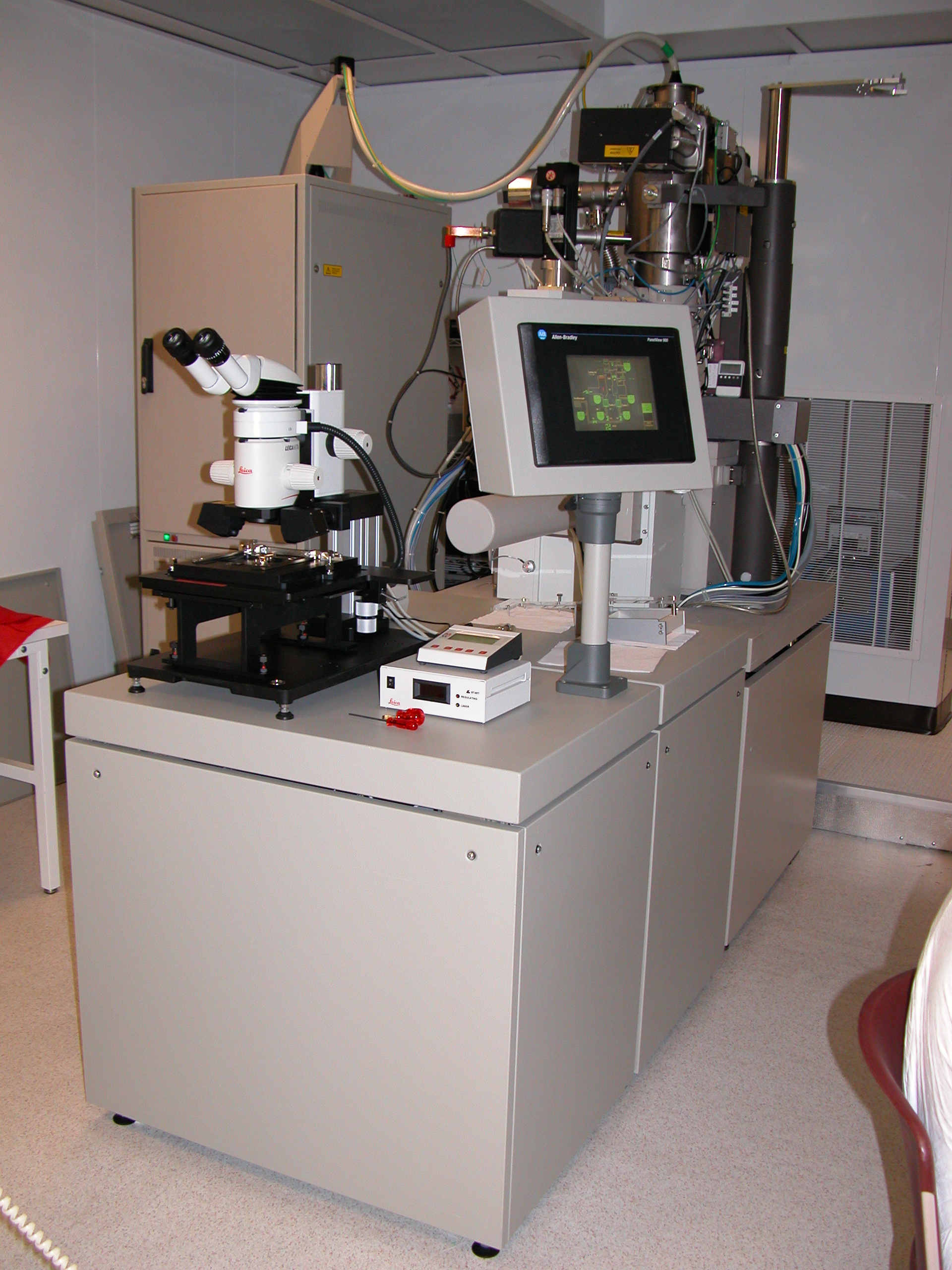
Below are a few recent photographs of the EBL lab space (February/March 2005).

UPDATE
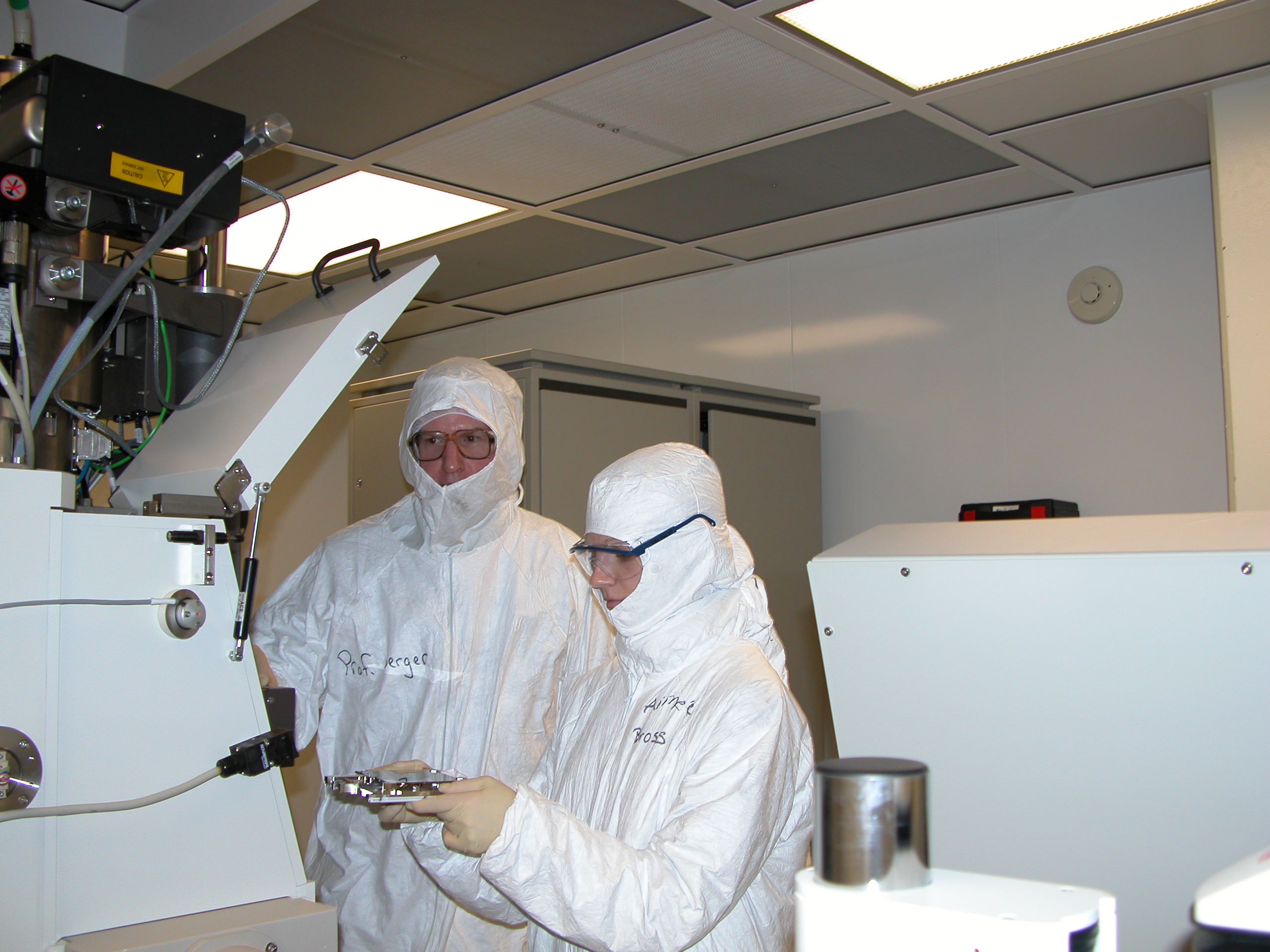
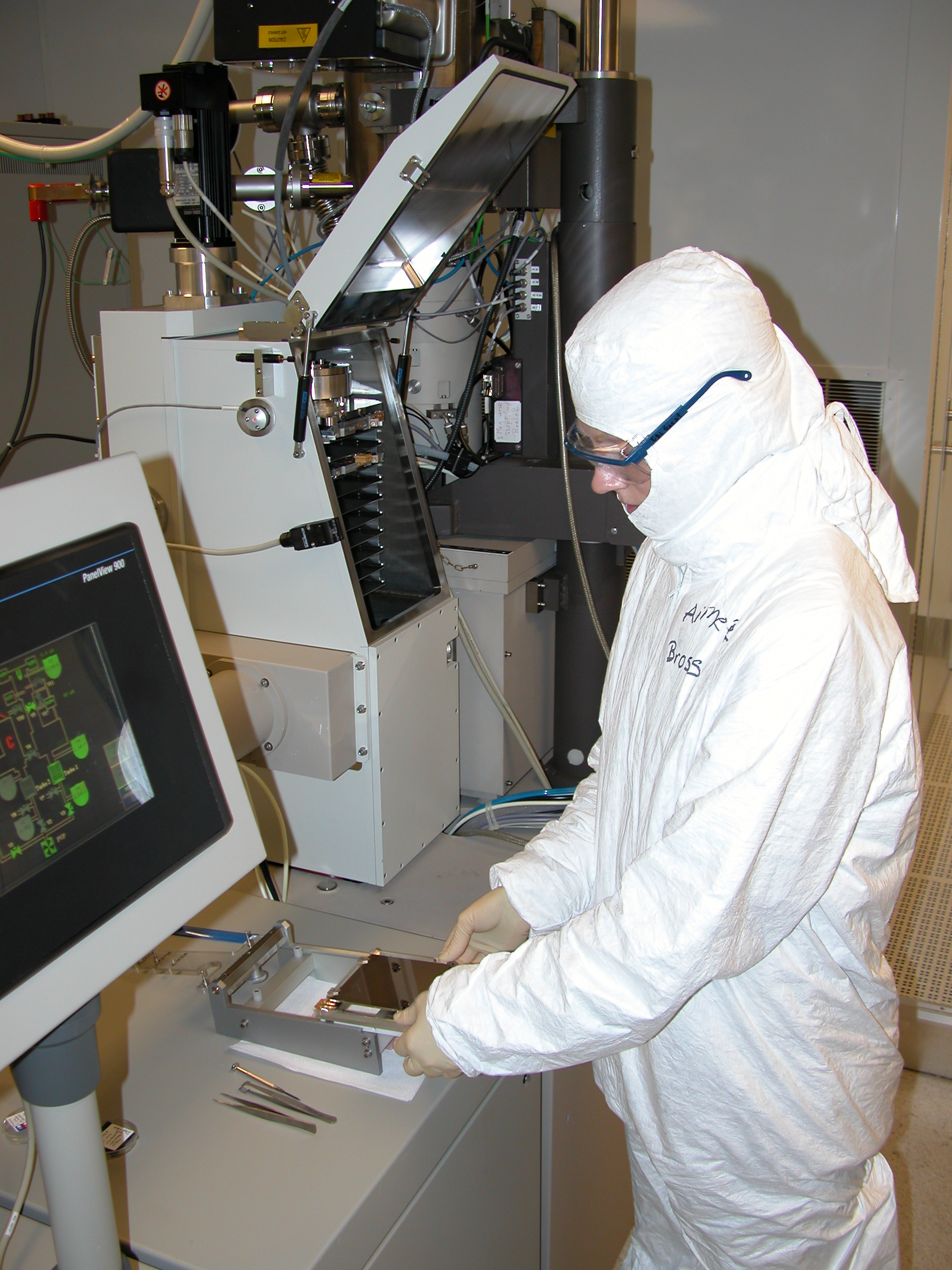
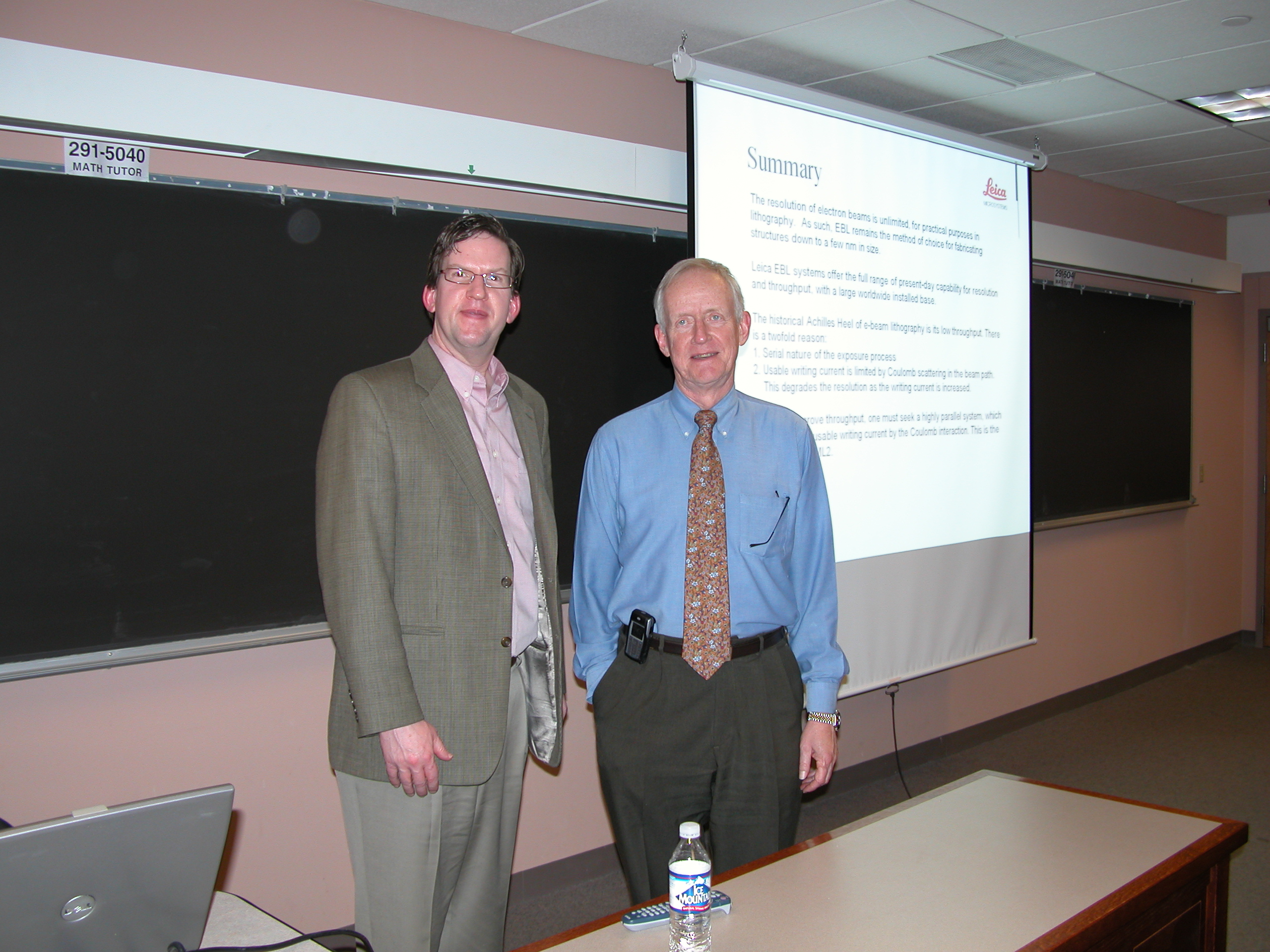
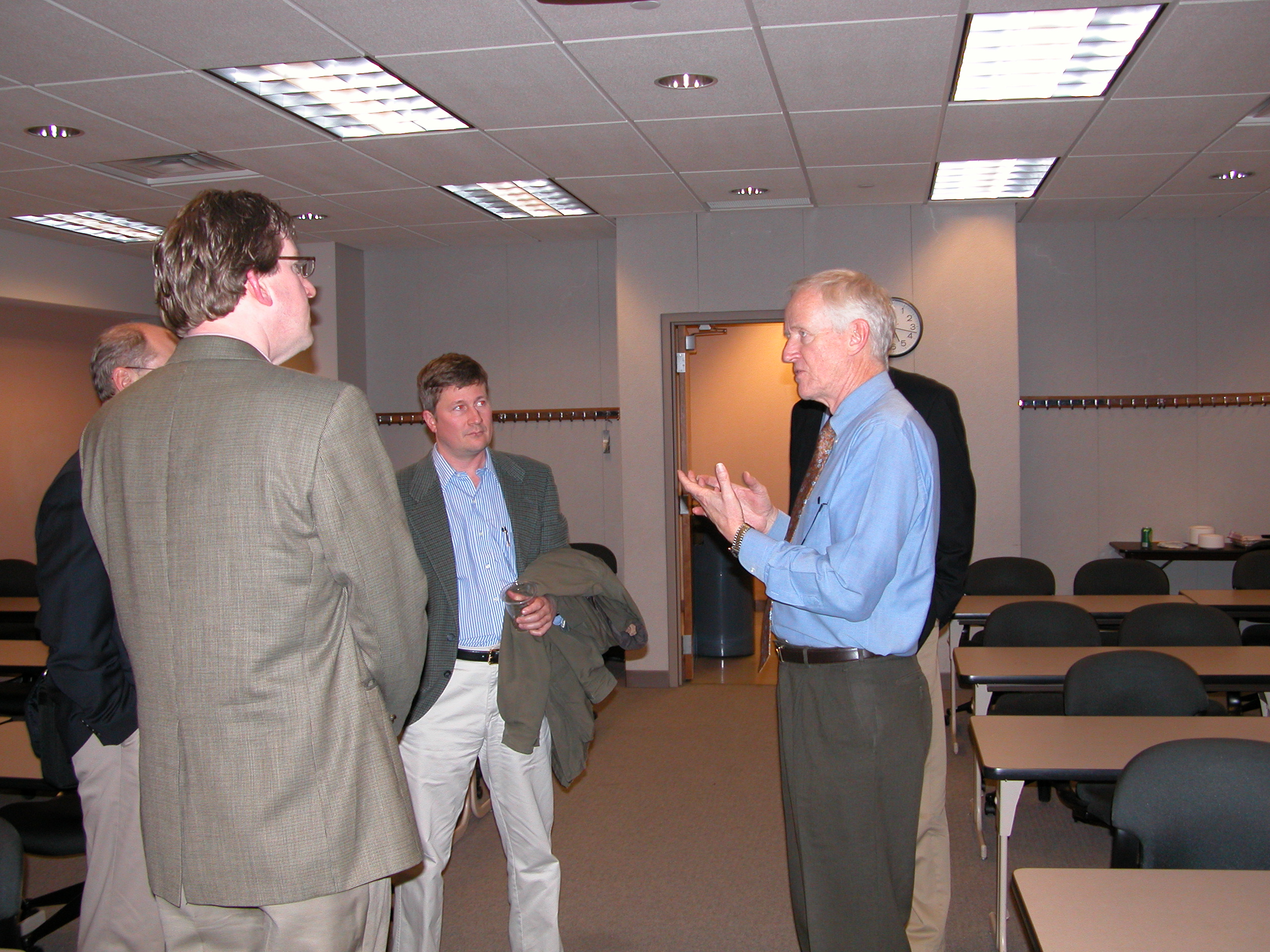
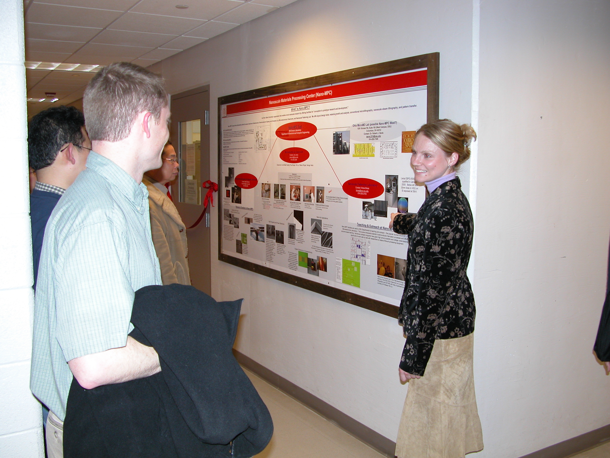
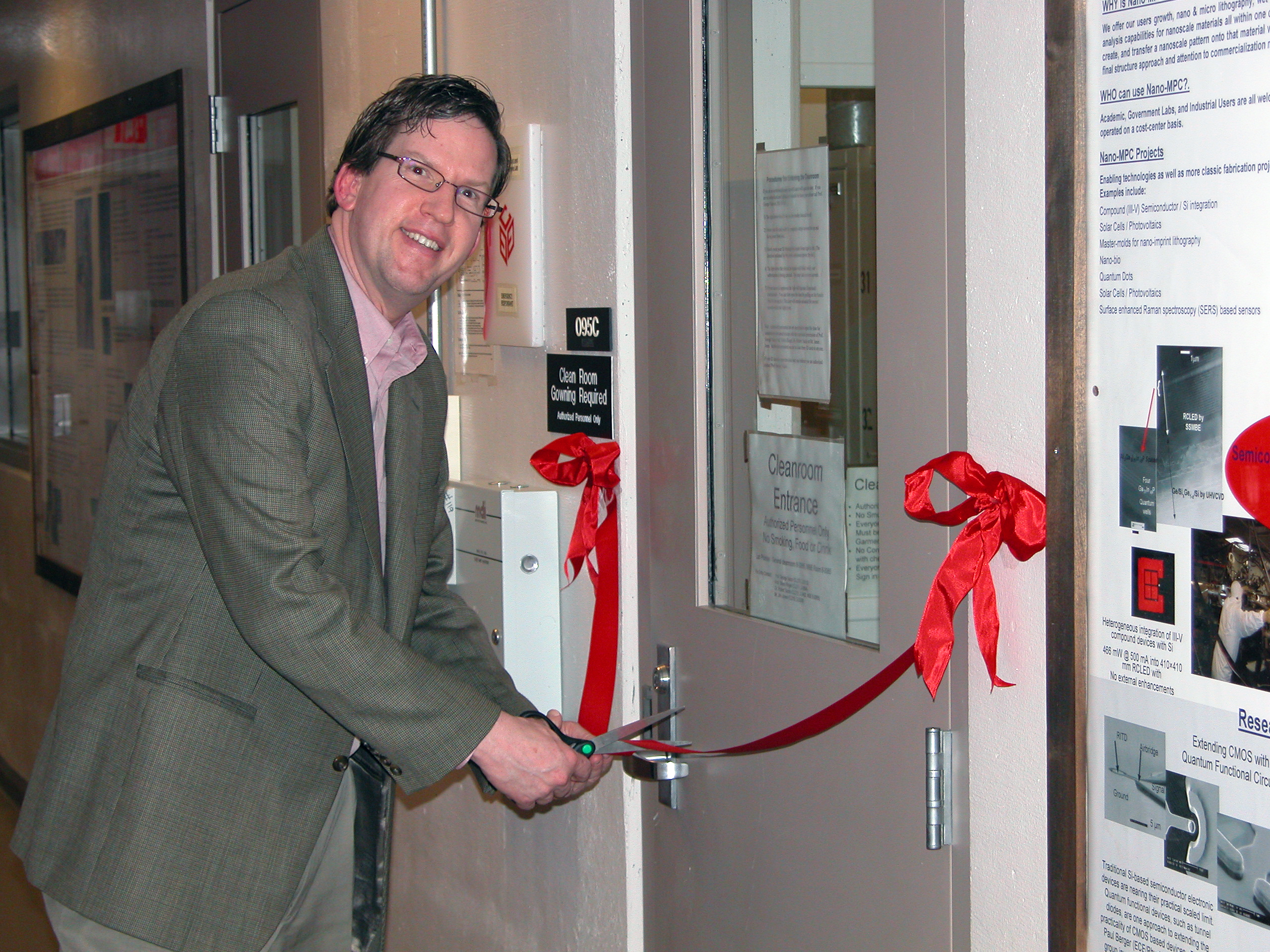
Below are a few images from the April 3, 2006 Kickoff Celebration.
 Return to
Paul R. Berger's homepage
Return to
Paul R. Berger's homepage
Send suggestions or comments to
pberger@ieee.org.
Last updated September 17, 2007.


